

 Previous
LEAVE A REPLY
Your email address will not be published.Required fields are marked *
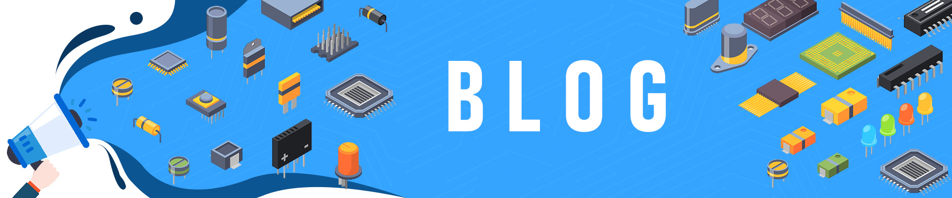
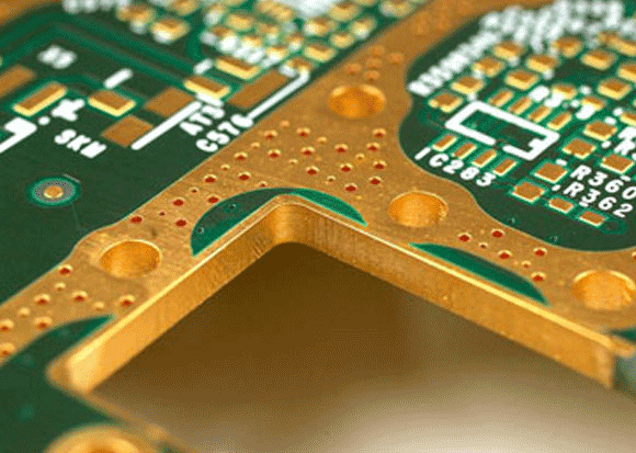
What is PCB Surface Finish? Normally, it means the coating applied on a bare PCB, to protect the copper from corrosion, and ensure components can be soldered onto pads.
Normally, the "PCB surface finish" means the coating applied on a bare PCB, to protect the copper, which is the main material of electronic circuit/wires, from corrosion, besides, the "surface finish" need to ensure that the electronic components can be easily and firmly soldered onto pads.
What's the most popular used PCB surface finish Method?
Nowadays, the most popular process for PCB surface finish used:
● ENIG
● Hasl Lead-Free
● OSP
1. ENIG PCB
The ENIG means Electroless Nickel Immersion Gold, it is a double-layer metallic coating, with nickel that acts both as a protective barrier to the copper, and a surface on which the components are welded. There 2 steps for this processing "EN", which means depositing nickel on the palladium-catalyzed copper surface; and the "IG" means Immersion Gold adhesive to the nickel-plated areas, to protect the nickel until the soldering process.
As there GOLD on the surface, it shows golden yellow on the pads, actually if you are patient enough, you can really get gold from the surface…
Actually, this production step is dangerous and high-cost, although the gold layer is very thin and takes little gold, the related instruments are expensive, and the regulation is strict, or it would be dangerous. So, actually many PCB factories do not do this by themselves, but send all the PCBs to special ENIG factories for this, to share the instruments. ENIG coating is hard and durable. It also has a long shelf life, lasting for years. However, expensive.
2. Hasl Lead-Free
Actually, the Hasl surface finish once the most popular, but as more and more countries restrict on Hasl, or ROHS requests, it is now all PCB factories stopped the Hasl processing, but use the Hasl Lead Free.
Of course, the most advantage for this Hasl Lead Free processing is its lower price, 20% lower. And the disadvantages: uneven surface and not so stable, which is not good for small size/ high precision components such as BGA/ QFN.
In Hasl Lead Free processing, submerge the boards in a bath of molten tin/ lead alloy, and then removing excess solder using "air blades", which blow hot air through the plate surface.
3. OSP(Organic Solderability Preservatives)
Organic Solderability Preservatives refers to a layer of organic finish generated on clean and bare copper by adsorption. This organic finish is capable of stopping copper from being oxide, thermal shock, or moisture. However, at subsequent welding temperatures, the protective film easily removed by the flux, so that the exposed clean copper surface can be immediately combined with the molten solder to form a solid solder spot in a very short time. The optimal storage conditions are relative humidity (30-70% RH), moderate temperature (15-30%), not sunlight exposure.
For OSP, the most advantage is its flat surface while cost-effective in mass production(compares to ENIG), suitable for mass production while high surface requests. Its shortcomings include a variety of actual recipes and performance. The protective film is extremely thin and prone to scratches (or bruises) and must be carefully manipulated and transported. That is, the thin film may get destroyed in the shipping/ packaging.
4. Makerfabs suggestions on PCB surface finish:
1. For projects with none small size components, normally standard consume electronics products → Hasl Lead Free
2. With small size components, BGA/ QFN/ 0201, OSP or ENIG
3. For mass production, ENIG is high cost
PCB Surface Finish Suggestions:
| Surface Finish | Cost | Surface Planeness | Stability | Appearance |
| Hasl Lead Free | Cheap | Bad | Bad | Middle |
| OSP | Middle | Good | Middle | Bad |
| ENIG | HIGH | Good | Good | Good |
@all, if you have any request on PCB/ PCBA manufacturing, pls drop us an email to service@makerfabs.com


