

 Previous
LEAVE A REPLY
Your email address will not be published.Required fields are marked *

Introduction: Why the Assembly Layer Matters
While copper traces define the electrical connectivity of a PCB, it is the assembly layer that determines whether a design can be transformed into a reliable, manufacturable product. At Makerfabs, we regard the assembly layer as the bridge between design intent and high-quality PCB assembly (PCBA), ensuring precision, repeatability, and traceability throughout the production flow.
I.What the Assembly Layer Defines
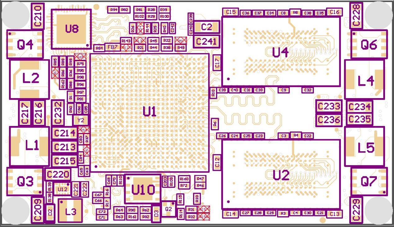
A PCB (Printed Circuit Board) is constructed from multiple layers that are vertically oriented relative to the board's surface. For example, a 2-layer board consists of a top and a bottom layer, while a 4-layer board includes a top layer, two inner layers, and a bottom layer.
At the core of each layer lies an insulating substrate—typically FR4 (Fire Retardant Version 4). This material is made of epoxy-saturated fiberglass combined with Teflon-based elements. Standard PCBs also feature solder masks on their copper surface layers, which may extend to both the top and bottom layers. These masks are applied as either liquid coatings or solid sheets.
Key Components of PCB Layers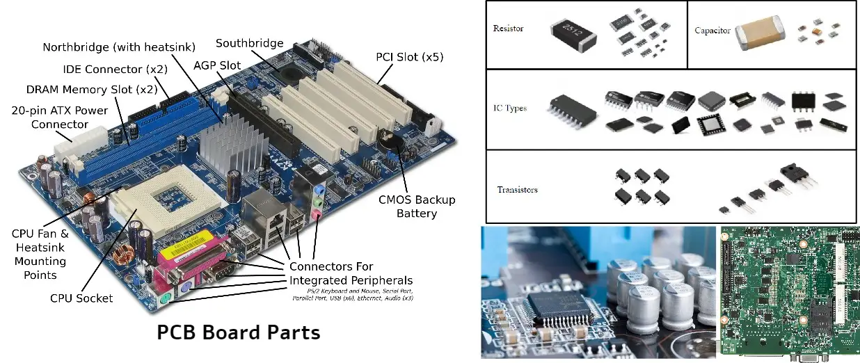
1. Dielectric Materials
· Dielectric materials serve two primary functions in a PCB:
· Separation of signals: They isolate signals between adjacent layers, preventing interference.
Impedance control: They ensure constant impedance across a wide frequency range, crucial for signal integrity.
2. Copper
Copper is essential in PCBs for its role as a conductor of electricity. It influences how the PCB handles current and power dissipation. The quality of copper in a board affects several factors such as impedance, thermal conductivity, and the overall stability of the PCB. The thickness and length of copper traces further enhance the board’s integrity and performance.
3. Trace Dimensions
Trace dimensions are fundamental to defining the mechanical layout of the PCB. They provide the necessary measurements for assembly and component placement, ensuring the correct locations for routing and positioning.
Types of PCB Layers
1. Mechanical Layers
The Mechanical 1 layer is essential for defining the physical dimensions of the PCB. Manufacturers rely on this layer to cut the PCB from raw materials. Other mechanical layers may be added to specify tooling requirements or other mechanical details, although not all designs require these additional layers.
2. Kept-Out Layers
Kept-out layers help define areas that must remain clear of components or traces. For example, you may use a kept-out layer to keep components a certain distance away from the edge of the PCB. These layers are used within design software to ensure boundaries are respected, but are not part of the final manufacturing files.
3. Routing Layers
Routing layers facilitate the interconnection of PCB components, with traces running across the upper, lower, and inner layers of the PCB. These layers require careful design and must be included when submitting the board for fabrication. They define the connections between components and the pads where the components will be mounted.
4. Ground and Power Planes
Ground and power planes are copper layers that provide stable connections to GND (ground) and the power supply. These planes help distribute power efficiently across the PCB and can enhance performance by reducing signal interference and noise.
5. Split Planes
Split planes allow different voltage potentials to be distributed across the same copper layer. For example, one section of the board may be connected to +5V, while another section receives -5V. This feature is particularly useful in designs requiring multiple voltages. Careful design is necessary to avoid issues with signal integrity, especially when using split ground planes.
6. Overlay/Silkscreen Layers
Silkscreen layers apply text designators (e.g., component labels) to the top and bottom of the PCB. These text labels help during assembly and testing, especially when debugging. In addition to part labels, the silkscreen may include other identifiers such as the board’s serial number or version.
7. Solder Mask Layers
Solder masks provide a protective coating on the PCB’s copper layers, preventing unintended short circuits and protecting against environmental damage. These masks are typically applied to the upper and lower layers, with openings for the pads that require soldering.
8. Solder Paste Layers
Solder paste layers are used for surface-mount components. The paste helps solder the component pins to the PCB by providing a conductive medium. Separate files are created for the solder paste to ensure proper placement on the pads.
How to Determine the Number of Layers in a PCB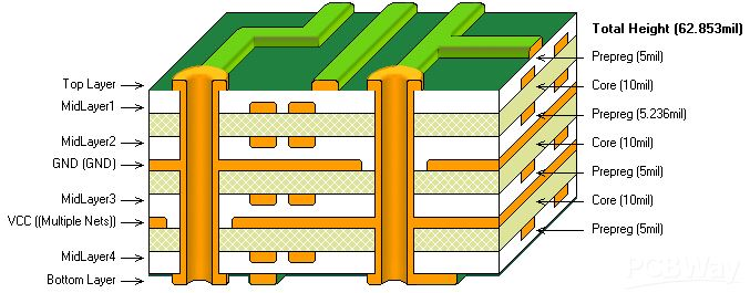
The number of layers in a PCB depends on the complexity of the design. Here’s a guide to help determine the right number of layers for your project:
1. 1 or 2-Layer PCB: Ideal for simple, low-density designs or breakout boards. These are often used for low-speed circuits or less complex applications.
2. 4-Layer PCB: This is a commonly used option for small boards, simple microcontroller designs, or baseboards. It offers a good balance between complexity and performance.
3. 6-Layer PCB: Suitable for more complex, high-density designs, often used in high-speed circuits or larger boards like PC motherboards.
4. 8-Layer PCB: Typically used in compact devices with minimal spacing, such as wearables, and high-performance applications like communication backplanes.
5. 10-Layer PCB: This layer count is optimal for high-density designs, offering ample room for power and ground planes, as well as various signal layers.
6. 12-Layer PCB: Ideal for industrial applications requiring multiple stable ground and signal layers.
Steps to Design Your PCB Layout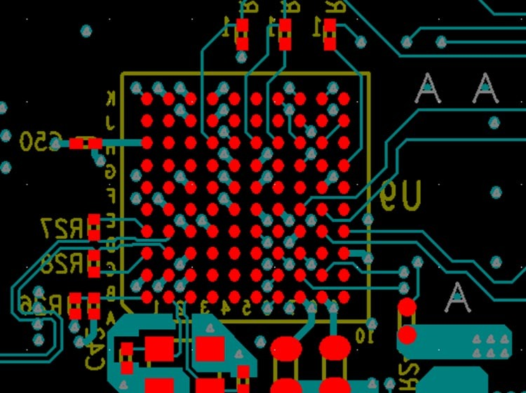
1. Start with the Upper and Lower Layers: For high-speed designs, consider adding internal layers to manage the signals effectively.
2. Place Signal Layers in Order: The most common configuration is placing the ground (GND) layer as the second layer to shield high-speed signals.
3. Establish Signal Layers and Density: Determine the signal layer density based on the type of components and connections required in your design.
II. Makerfabs Workflow: Assembly Layer in Action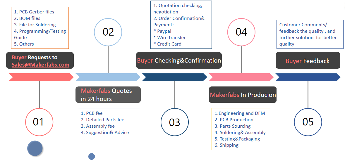
Data Verification & Pre-production Review
Engineering teams review Gerber files, BOM, and assembly drawings for completeness. Missing or ambiguous assembly layer details are resolved before procurement and fabrication.
Component Sourcing & Incoming Inspection
All components are sourced per BOM specifications. Each lot is verified for package type, batch number, and footprint compatibility against the assembly layer.
First Article Inspection (FAI)
Before volume assembly, a first board is built and thoroughly inspected for placement accuracy, polarity, and soldering quality. Approval at this stage locks the process for mass production.
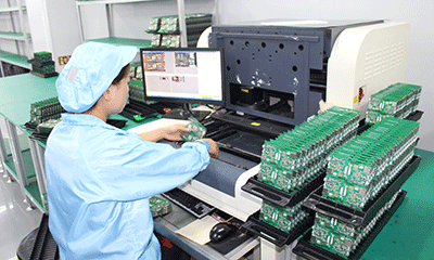
SMT, THT, and Automated Optical Inspection (AOI)
SMT components are placed with high-speed pick-and-place machines guided by the assembly layer data. AOI systems validate solder joint quality, while THT parts undergo wave soldering or manual soldering as required.
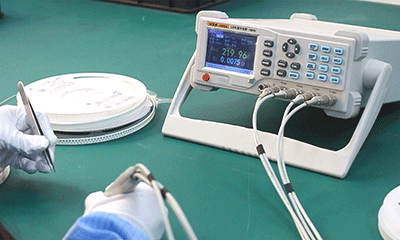
Functional Testing & Validation
Dedicated test jigs are designed based on assembly layer outputs. This ensures 100% functional coverage, from simple connectivity to complex firmware validation.
At Makerfabs, we ensure that every product—from prototypes to mass production—benefits from a robust assembly layer workflow, letting our partners focus on innovation while we secure manufacturing excellence.


