

 Previous
LEAVE A REPLY
Your email address will not be published.Required fields are marked *
In the world of PCB design, selecting the right components and optimizing their layout can make or break the functionality, reliability, and manufacturability of the board. Poor component selection can lead to issues like signal integrity problems, overheating, and difficulty in assembly, all of which delay product development and increase costs. Conversely, effective design practices ensure high performance, streamlined manufacturing, and a product that meets the functional and environmental needs of the application. In this guide, we'll explore the best practices for component selection and PCB layout optimization, ensuring your designs are both functional and cost-effective.
I. The Importance of Component Selection in PCB Design
Component selection is the first and most critical step in designing any PCB. The choice of components impacts the overall performance, longevity, and efficiency of the circuit.
Meeting Functional Requirements
The core principle behind component selection is aligning the component's properties with the project's functional requirements. A functional block diagram, which outlines all the necessary functions in a system, is a helpful tool to guide the selection process.
For example, if you need to convert a 12V input to a 24V output, a boost converter is a natural choice. But in selecting the specific boost converter, factors like efficiency, output voltage range, and input current need to be carefully considered to meet the exact needs of the application.
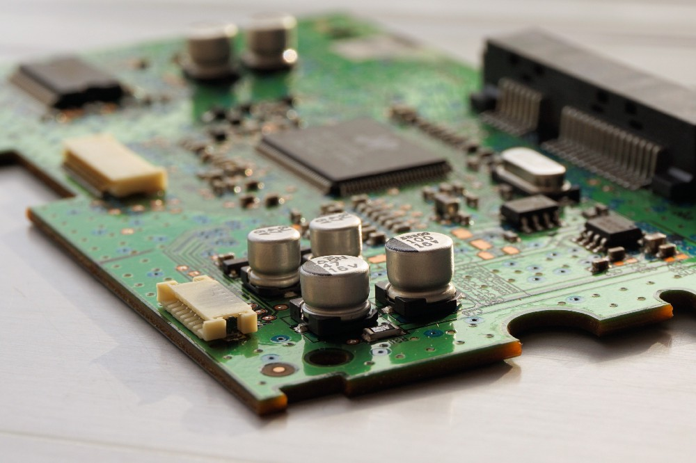
Electrical and Physical Criteria
When selecting a component, it is vital to ensure it meets the electrical criteria such as voltage, current, and frequency. Additionally, physical criteria, like size, packaging type, and mounting style (SMD vs. through-hole), must also align with the available space on the PCB and manufacturing processes.
Key Steps in Component Selection:
II. Efficient Component Layout on Your PCB
Once you’ve chosen the right components, the next challenge is laying them out efficiently on the PCB. A well-thought-out layout can significantly improve the performance and ease of assembly, reducing production time and cost.
Best Practices for Component Placement
Here are some key guidelines for PCB layout optimization:
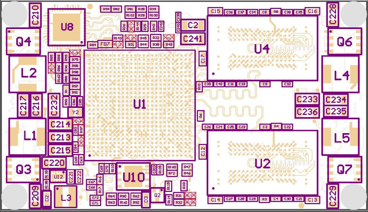
Grouping Components by Function
It’s essential to group components logically according to their functionality. For instance, power supply components should be grouped together in one section, while analog components and digital components should have dedicated areas to minimize interference. Proper grouping simplifies the routing process and improves the PCB's overall performance.
Managing EMI (Electromagnetic Interference)
EMI can cause signal distortion or data loss in sensitive components. Proper shielding and keeping high-frequency circuits away from low-frequency circuits will mitigate these issues. Use ground traces and copper pours as shields wherever necessary.
III. DFM & DFT: Design for Manufacturability and Testing
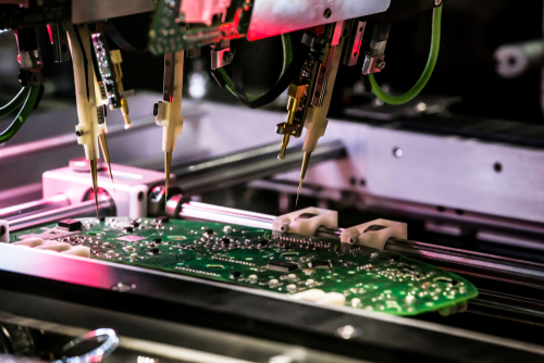
DFM (Design for Manufacturability) and DFT (Design for Testing) are essential considerations during PCB design to ensure that your board is not only functional but also easy to manufacture and test.
Design for Manufacturability (DFM)
To optimize DFM, ensure that:
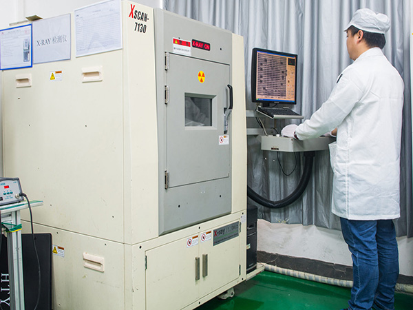
Design for Testing (DFT)
Testing your PCB design is crucial, and DFT involves designing the PCB so that it is easy to test. Here’s how to achieve it:
IV. Advanced Considerations for Complex Designs
When dealing with high-speed designs, complex signal routing, or advanced applications, additional considerations come into play.
Signal Integrity and Impedance Matching
For high-frequency designs, maintaining signal integrity is critical. Here’s how you can optimize it
Choosing Newer Parts
As component obsolescence can be a significant issue, always try to use newer parts that meet the same functional requirements as older components. Newer components tend to have:
V. Testing and Validation Before Production
Before committing to full-scale production, prototyping and testing the design is essential to catch any issues early.
Prototyping
Creating prototypes is an essential part of the design process. It allows you to:
Iterative Design
PCB design is an iterative process. Based on test results, make modifications to the design and test again. This process continues until the final product meets all functional, performance, and manufacturability requirements.
At Makerfabs, we understand that selecting the right components and optimizing the layout are essential steps in ensuring a successful PCB design. With years of experience in electronics manufacturing, we provide expert guidance in selecting the best components for your project and designing optimized layouts for both small-batch prototyping and mass production.
We are committed to providing high-quality PCB assembly services, ensuring your boards are designed for durability, performance, and efficiency.


