Makerfabs National Day & Mid-Autumn Festival Holiday Notice: 01/10/2025-07/10/2025


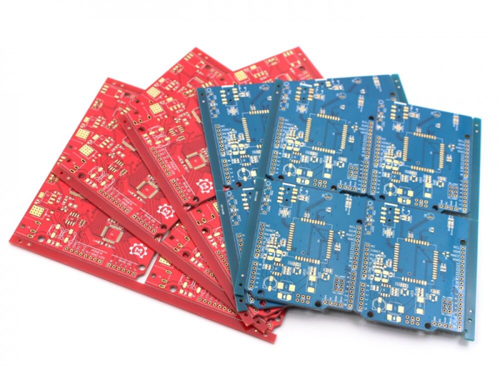

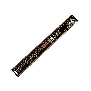
The way for the makers& startups to get the PCBs for prototyping or trial-production, at a low price while the production and quality control follows all industrial standards.
How Does PCB Prototyping Service work?
1. Choose your options above, include the PCB size, layers, color, finish, etc.
2. Verify that your Gerber files comply with all specs, and upload them.
3. Add to Cart. The system will calculate the final price for you.
For bigger quantities, more layers, special options, tests, panels, discounts, or combined with our other services, contact us directly at sales@makerfabs.com.
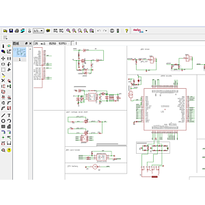
Gerber Files:
pcbname.GTL: Top layer
pcbname.GBL: Bottom layer
pcbname.GTS: Solder Stop Mask top
pcbname.GBS: Solder Stop Mask Bottom
pcbname.GTO: Silk Top
pcbname.GBO: Silk Bottom
pcbname.TXT: NC Drill
pcbname.GML: Mechanical layer
Note:
1. Note that Gerber files must be RS-274x format
2. Drill file(pcbname.TXT) should be Excellon format, and make sure it includes drills size and position data
3. Besides the production Gerber files, We also accept PCB files generated by Eagle, Altium Designer, PADS
4. Please leave a comment in the order for special requirements
Specs:
Layers 1/2/4
PCB Material FR-4
Thickness Tolerance (t≥1.0mm) ± 10%
Thickness Tolerance (t<1.0mm) ± 0.1mm
Insulation Layer Thickness 0.075mm--5.00mm
Minimum PCB track 6mil
Minimum Track/Vias Space 6mil
Minimum pads Space 8mil
Minimum silkscreen text size 32mil
Inner Layer Copper for 4-layer PCB 17um
Drilling Hole (Mechanical) 0.3mm—6.35mm
Finish Hole (Mechanical) 0.8mm—6.35mm
Drill Diameter Tolerance (unplated) 0.05mm
Drill Diameter Tolerance (plated) 0.1mm
Outline Tolerance (Mechanical) ±0.20mm
Aspect Ratio 8:1
Solder Mask Type Photosensitive ink
SMT min Solder Mask Width 0.2mm
Min Solder Mask Clearance 0.2mm
Solder Mask Thickness 15um
Documents:
2 Layer PCB CAM Job File
4 Layer PCB CAM Job File
2 Layer PCB Design Rules and CAM for Eagle PCB
Write Your Own Review